FIRE EYE NANO
Home
About Us
Products
Support
News
Contact Us
EN
中文
English
Search
Home
/
Products
/
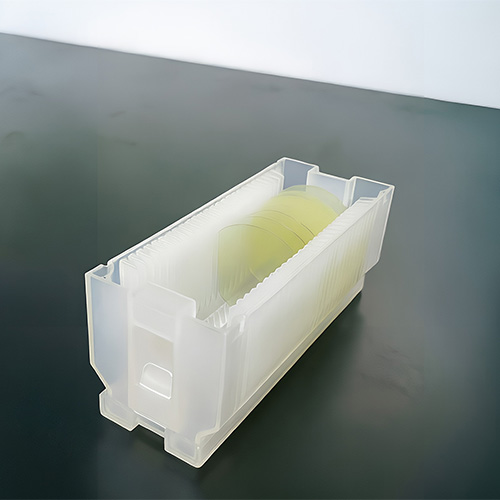
Monolayer MoS2 Wafer 2-inch
Monolayer MoS2 Wafer 2-inch
FE-MoS2
Model
FE-MoS2-2i
Category
FE-MoS2
Summary
Monolayer MoS₂ possesses a direct bandgap of approximately 1.8 eV and a thickness of about 0.6 nm.
It can be utilized to fabricate transistors with ultra-short channels, as well as photodetectors and chemical sensors.
Details
—— Characterization ——
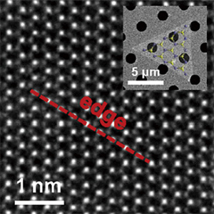
HADDF-STEM Image
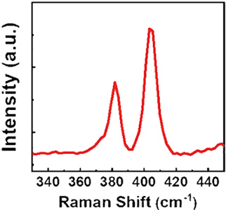
Raman Spectrum
—— Specifications ——
FE-MoS2-Al2O3
FE-MoS2-SiO2
Wafer Size
2-inch
MoS
2
Coverage
> 99 %
Monolayer Percent
> 99 %
Substrate
Sapphire
SiO
2
/ Si
Domain Size
> 50 μm
> 30 μm
Growth method
CVD